Earlier Defect Identification in Semiconductor Packaging: Why Process Control Is Moving Upstream
Semiconductor Process Control: Why Earlier Defect Identification Matters
Key Takeaways
- Semiconductor process control identifies manufacturing variation before defects become costly.
- Earlier inspection reduces scrap, rework and production downtime.
- Inspection and metrology complement each other to improve manufacturing stability.
- Semiconductor process control helps manufacturers achieve higher yield and better product quality.
Introduction to Semiconductor Process Control
Semiconductor process control is the foundation of modern semiconductor manufacturing. Semiconductor process control allows manufacturers to identify process variation before defects occur, helping engineering teams improve yield, reduce scrap and maintain consistent product quality.
However, semiconductor packaging continues to become more complex. Devices are becoming smaller, feature sizes are shrinking and manufacturing tolerances are becoming increasingly tight. As a result, manufacturers have far less room for process variation than ever before.
Advanced packaging technologies such as wafer-level packaging (WLP), fan-out wafer-level packaging (FOWLP), 2.5D integration, 3D IC packaging and heterogeneous integration all require tighter manufacturing control. Therefore, inspection is no longer limited to the end of the production line.
Instead, manufacturers are moving inspection and metrology upstream. By applying semiconductor process control throughout every critical manufacturing stage, engineering teams can detect variation earlier, minimise rework and improve overall production efficiency.
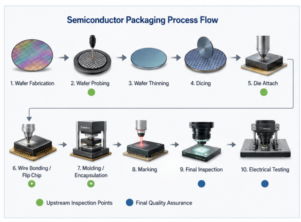
Why Semiconductor Proces
Semiconductor process control throughout semiconductor packaging from wafer inspection to final electrical testing.
Every manufacturing process introduces variation. Some variation is acceptable. However, uncontrolled variation eventually becomes a manufacturing defect.
Consequently, manufacturers monitor each critical process rather than relying solely on final inspection. Earlier visibility allows engineering teams to make process adjustments before quality problems affect production.
| Traditional Manufacturing | Semiconductor Process Control |
|---|---|
| Defects discovered during final testing | Defects identified immediately after each process |
| Higher scrap costs | Lower manufacturing costs |
| Reactive troubleshooting | Preventive process monitoring |
| Equipment drift often goes unnoticed | Continuous monitoring of equipment performance |
| Reduced production yield | Improved manufacturing yield |
❓ Why not wait until final inspection?
Every manufacturing process adds value to a semiconductor device. Therefore, discovering a defect at the end of production means the manufacturer has already invested materials, labour, machine time and production capacity into a product that may ultimately be scrapped.
Earlier inspection allows manufacturers to stop defects from progressing further through production. As a result, manufacturing costs decrease while production yield improves.
Why Earlier Defect Identification Supports Semiconductor Process Control
Every semiconductor package passes through numerous value-added manufacturing stages before reaching final electrical testing.
Typical production processes include:
- Incoming wafer inspection
- Wafer probing
- Wafer thinning
- Dicing
- Die attach
- Wire bonding or flip-chip assembly
- Molding and encapsulation
- Laser marking
- Final optical inspection
- Electrical testing
Each manufacturing stage increases the overall value of the semiconductor package. Consequently, identifying defects earlier provides significant cost savings while supporting more effective semiconductor process control.
💡 Engineering Insight
Process variation almost always appears before product defects. Therefore, engineers monitor process stability rather than waiting for quality failures. This proactive approach improves yield, reduces downtime and strengthens semiconductor process control.
Why Modern Semiconductor Packaging Requires Better Semiconductor Process Control
Today’s semiconductor packages are significantly smaller and more complex than previous generations.
For example, manufacturers now work with ultra-thin wafers, fine-pitch wire bonding, high-density redistribution layers, chiplet architectures and advanced package substrates.
Because these technologies have tighter manufacturing tolerances, even small changes in temperature, bonding force, alignment or material properties can affect product quality.
Therefore, semiconductor process control has become a core manufacturing strategy rather than simply a quality assurance activity.
How Metrology Supports Semiconductor Process Control
Inspection identifies defects after they occur. Metrology, on the other hand, measures manufacturing variation before defects develop.
Together, inspection and metrology provide the foundation of effective semiconductor process control, allowing manufacturers to monitor process capability, equipment performance and dimensional accuracy throughout production.
❓ Inspection vs. Metrology – What’s the Difference?
| Inspection | Metrology |
|---|---|
| Identifies visible defects | Measures process variation |
| Pass / Fail decision | Quantitative measurement |
| Quality verification | Process optimisation |
| Detects defects | Prevents defects |
Typical metrology measurements include:
- Wafer thickness
- Surface topography
- Critical dimensions
- Package warpage
- Die shift
- Coplanarity
- Surface roughness
Using Process Data for Continuous Improvement
Modern inspection systems generate far more than simple pass or fail results.
Every inspection creates valuable production data that engineers can analyse to improve manufacturing stability.
When inspection systems are integrated with Statistical Process Control (SPC), manufacturers gain greater visibility into process performance.
Typical metrics include:
- Process capability (Cp/Cpk)
- Equipment drift
- Yield trends
- Lot-to-lot consistency
- Defect rates
- Machine variation
- Production stability
💡 Engineering Insight
Successful semiconductor manufacturers rarely wait for yield loss before taking action. Instead, they monitor production trends continuously, allowing engineers to identify subtle process changes long before defects become widespread.
Semiconductor Process Control for Advanced Packaging
Emerging semiconductor technologies continue to increase manufacturing complexity.
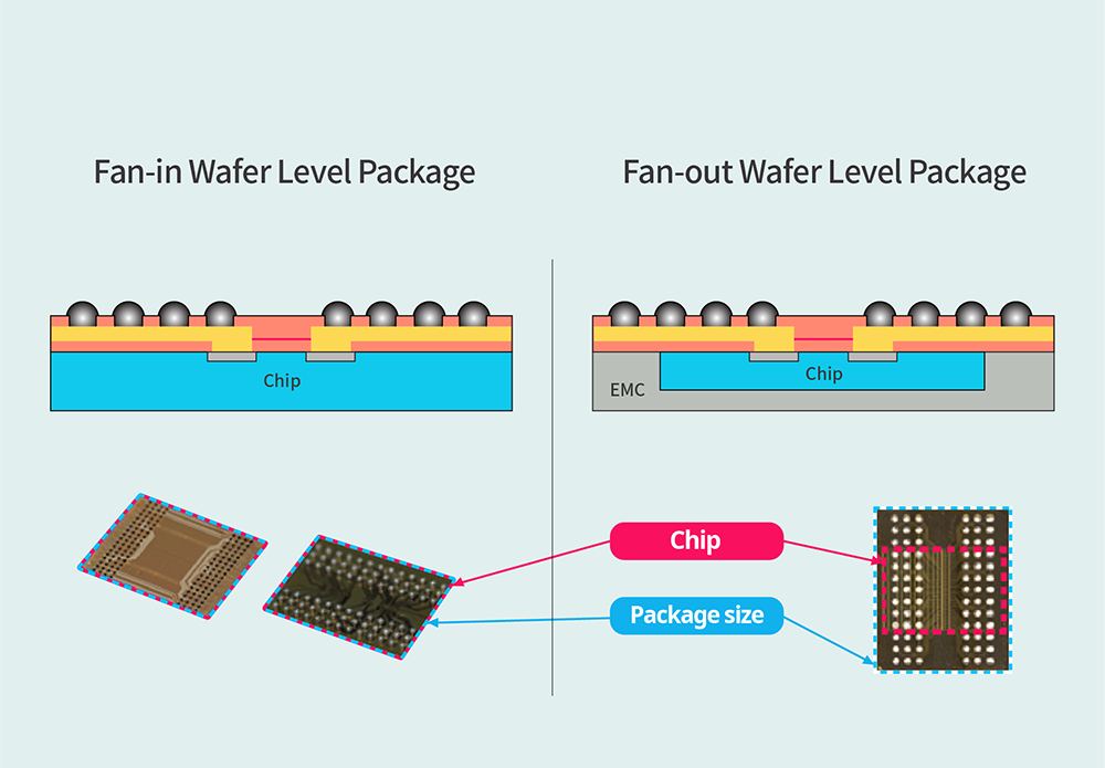
Applications such as Fan-Out Wafer-Level Packaging (FOWLP), 2.5D integration, 3D IC packaging, chiplet architectures and heterogeneous integration all require tighter process windows than traditional semiconductor packages.
As package dimensions shrink and interconnect density increases, even small manufacturing deviations can affect product reliability.
For this reason, semiconductor process control has become an essential manufacturing strategy rather than simply a quality assurance activity.
📊 Did You Know?
Many semiconductor manufacturers inspect products multiple times throughout production rather than relying solely on final inspection. This layered inspection strategy helps improve yield while reducing the cost of poor quality.
Conclusion
Semiconductor process control is no longer limited to final inspection. It is a comprehensive manufacturing strategy that combines inspection, metrology and process monitoring to improve production quality throughout every stage of semiconductor packaging.
By identifying variation earlier, manufacturers can reduce scrap, minimise rework, improve equipment utilisation and maintain stable manufacturing processes. Earlier defect identification also enables faster root cause analysis and more effective continuous improvement.
As semiconductor packaging technologies continue to evolve, robust semiconductor process control will remain essential for delivering reliable products while maintaining competitive manufacturing performance.
Frequently Asked Questions
What is semiconductor process control?
Semiconductor process control is the continuous monitoring and measurement of manufacturing processes to identify variation before defects affect product quality and production yield.
Why is earlier defect identification important?
Earlier defect identification reduces scrap, minimises rework and prevents defective products from progressing through expensive downstream manufacturing processes.
What technologies support semiconductor process control?
Common technologies include Automated Optical Inspection (AOI), semiconductor metrology systems, X-ray inspection, Scanning Acoustic Microscopy (SAM), Statistical Process Control (SPC) software and precision measurement systems.
How does semiconductor process control improve manufacturing yield?
By monitoring manufacturing variation throughout production, engineers can identify process drift earlier, implement corrective actions quickly and prevent widespread yield loss.
Continue Exploring
Automated Optical Inspection (AOI)
Discover how AOI supports earlier defect detection and manufacturing quality.
Coming Soon
Semiconductor Metrology vs Inspection
Understand the difference between measuring process variation and identifying manufacturing defects.
Coming Soon
Wire Bond Inspection
Learn about common wire bond defects and inspection methods used during semiconductor packaging.
Coming Soon
Industry References
- SEMI International
- JEDEC Solid State Technology Association
- IPC – Association Connecting Electronics Industries
Explore More Semiconductor Insights
The QES Knowledge Centre provides educational resources covering semiconductor inspection, metrology, process control, failure analysis and advanced manufacturing technologies.
Browse related articles to learn how modern inspection and analytical solutions help manufacturers improve product quality, production efficiency and process stability.