Why Automated Optical Inspection (AOI) Is Critical for Semiconductor Packaging Quality
As semiconductor packages become increasingly compact and complex, ensuring consistent manufacturing quality has become more challenging than ever. Smaller feature sizes, finer interconnects, and higher production volumes leave manufacturers with little room for error.
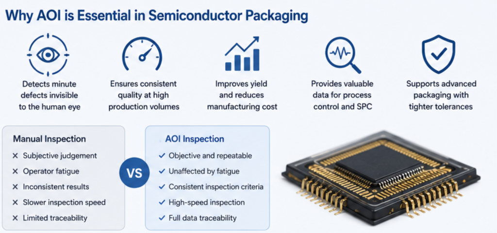
Traditional manual inspection methods are no longer sufficient to detect every defect with the speed and consistency required in modern semiconductor packaging. This has led to the widespread adoption of Automated Optical Inspection (AOI), a technology that enables manufacturers to inspect products quickly, accurately, and repeatably throughout the production process.
Rather than serving only as a final quality checkpoint, AOI has evolved into an essential process control tool that helps manufacturers maintain stable production, improve yield, and reduce manufacturing costs.
What Is Automated Optical Inspection?
Automated Optical Inspection (AOI) is a non-contact inspection method that uses high-resolution cameras, precision optics, controlled lighting, and advanced image processing algorithms to examine semiconductor devices for defects.
During inspection, captured images are compared against predefined design criteria or reference models. The system automatically identifies deviations that may indicate manufacturing defects.
Unlike manual inspection, AOI provides consistent inspection criteria regardless of production volume or operator experience.
Why Manual Inspection Is No Longer Enough
Manual visual inspection has traditionally played an important role in semiconductor manufacturing. However, today’s advanced packaging technologies present several challenges.
Modern packages feature:
- Fine-pitch wire bonds
- High-density interconnects
- Miniaturised components
- Ultra-thin wafers
- Multi-die assemblies
- Complex package geometries
Many of these features are difficult to inspect reliably using the human eye alone.
Manual inspection may also be affected by:
- Operator fatigue
- Subjective judgement
- Inconsistent inspection standards
- Slower inspection speed
- Limited traceability
As production volumes increase, these limitations become more apparent.
Where AOI Is Used in Semiconductor Packaging
AOI systems are commonly deployed at multiple stages throughout the semiconductor packaging process.
Wafer Inspection
AOI identifies defects such as:
- Surface scratches
- Particles
- Pattern defects
- Missing structures
- Surface contamination
Early inspection prevents defective wafers from progressing further into production.
Die Attach Inspection
After die placement, AOI verifies:
- Die position
- Alignment accuracy
- Rotation
- Epoxy coverage
- Missing dies
- Foreign particles
Accurate die placement is essential for reliable downstream assembly processes.
Wire Bond Inspection
Wire bonding remains one of the most critical assembly operations.
AOI evaluates:
- Bond placement
- Wire loop height
- Wire sweep
- Missing wires
- Lifted bonds
- Broken wires
- Bond deformation
Early detection allows process adjustments before yield is affected.
Molded Package Inspection
Following encapsulation, AOI inspects:
- Package cracks
- Flash
- Surface defects
- Marking quality
- Package dimensions
- Cosmetic defects
Inspection ensures that only conforming packages proceed to final testing.
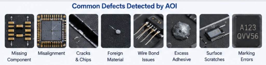
Common Defects Detected by AOI
Depending on the inspection stage, AOI systems can identify a wide range of manufacturing defects, including:
- Missing components
- Misalignment
- Surface contamination
- Cracks and chips
- Foreign material
- Scratches
- Incomplete bonding
- Excess adhesive
- Broken or missing wire bonds
- Marking errors
The ability to detect these defects consistently helps reduce both false rejects and escaped defects.
Benefits Beyond Defect Detection
Although AOI is primarily associated with defect inspection, modern systems provide much greater value.
Improved Process Consistency
Continuous inspection allows manufacturers to monitor process stability and identify equipment drift before it affects production yield.
Faster Root Cause Analysis
Inspection images and measurement data provide engineers with valuable evidence when investigating manufacturing issues.
Increased Throughput
Automated inspection supports high-volume production while maintaining consistent inspection quality.
Reduced Manufacturing Costs
Detecting defects earlier reduces:
- Scrap
- Rework
- Machine downtime
- Customer returns
- Cost of poor quality
AOI and Statistical Process Control
AOI systems generate valuable inspection data that can be integrated into Statistical Process Control (SPC).
Manufacturers can monitor:
- Defect trends
- Equipment performance
- Process capability (Cp/Cpk)
- Yield variation
- Lot-to-lot consistency
Rather than simply identifying defective products, AOI becomes part of a broader strategy for maintaining stable manufacturing processes.
Supporting Advanced Semiconductor Packaging
Emerging packaging technologies continue to place greater demands on inspection systems.
Applications such as:
- Fan-Out Wafer-Level Packaging (FOWLP)
- 2.5D integration
- 3D IC packaging
- Chiplet architectures
- Heterogeneous integration
require tighter dimensional tolerances and more sophisticated inspection capabilities.
AOI enables manufacturers to inspect increasingly complex package designs while maintaining production efficiency and consistent quality.
Selecting an AOI System
When evaluating an AOI solution, manufacturers typically consider several factors:
- Inspection accuracy
- Image resolution
- Throughput
- Lighting flexibility
- Ease of recipe creation
- False call rate
- Software capabilities
- Data integration with Manufacturing Execution Systems (MES) and Statistical Process Control (SPC)
The ideal system should balance inspection performance with production efficiency while supporting future manufacturing requirements.